Back to Peter's Guitar Effects Projects
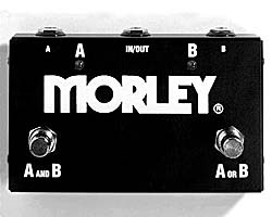
Bought a Morley© ABY splitter box for around $40. It's a A-B-Y splitter used to split a guitar signal into two channels for use in amplifier switching. It's a passive device except that it uses a 9V battery to power the LED's which show how the switching works.
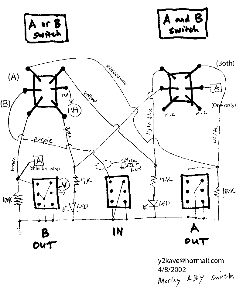
Here's a rough drawing of the existing Morley© switch circuit (click to enlarge)
My idea is to splice a version of the Anderton buffer circuit (a.k.a. "Spluffer") into the signal path to reduce the subtantial tone/volume drop which occurs when using this passive pedal. I figured that hey, if it already runs off of a 9V, it shouldn't be too tough to tough to incorporate the circuit.
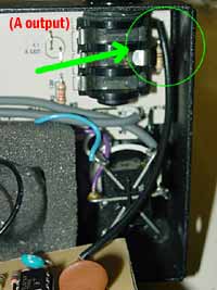
Here were some initial problems. The Morley© is pretty tightly packed already (see photo), so getting another battery in there, much less a board the size that Anderton proposes is impossible. So I realized that I would have to redraw the circuit to fit a smaller layout, as well as incorporate design features which would let the thing run off of a single battery power. Anderton's design runs off of a positive/negative supply which requires either a special dual polarity power supply (which you'll have to build yourself) or using two batteries.
Here's Anderton's original design:
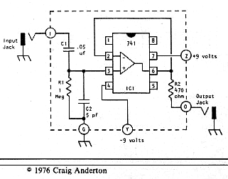
A fine design. Here's how it works:
C1: filters the input
C2: rolls off high frequencies
R1: sets the input impedance of the op-amp circuit
R2: sets the output impedance
The combination of high input impedance and low output impedance is supposed
to give the sound a kind of "boost" by allowing a guitar's signal
to pass more easily through an effects chain.
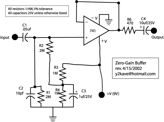
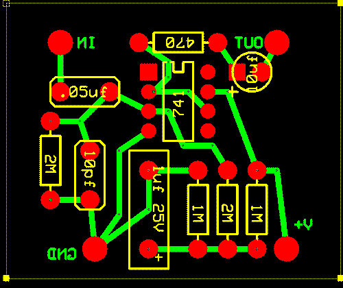
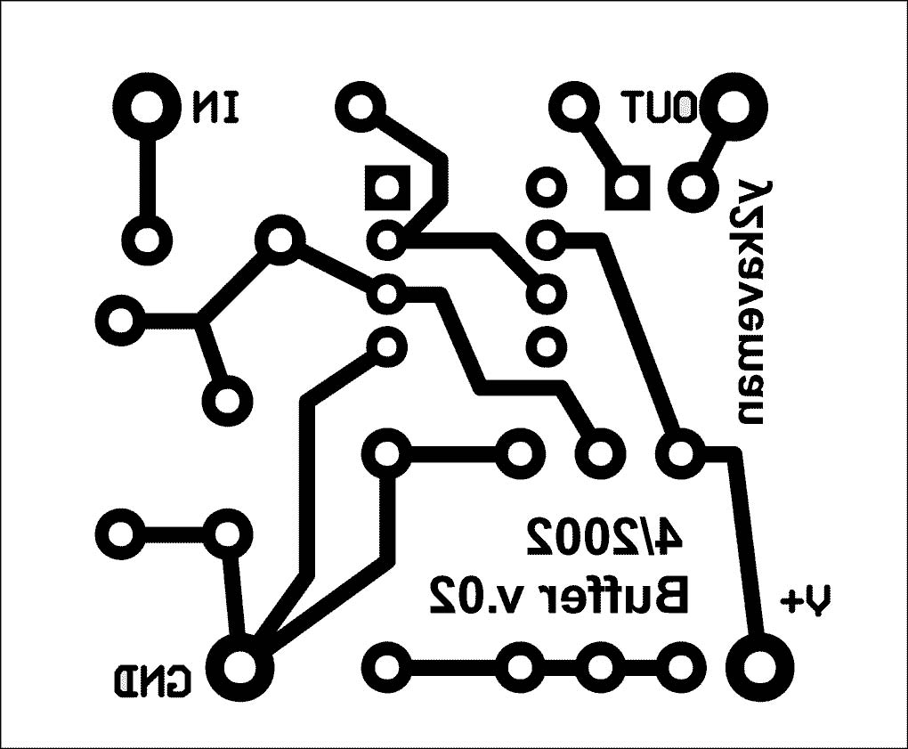
I designed the circuit below using the principles of Anderton's design. I added a single-battery type power supply for the circuit similar to that of the power supply in the MXR Distortion+ circuit. Here, R3 and R4 form a voltage divider, and provide a bias voltage of 4.5V to the non-inverting (+) side of the op-amp. The input impedance is set here by R1 and R2, resulting in an input impedance of about 1M. Capacitor C4 was added to work with the existing Morley circuit in blocking DC to reduce switching pops and clicks. Everything else is the same.
1. I designed the circuit using the free software from ExpressPCB. Only problem with this software, the pads it makes for its pre-built components (resistors, capacitors, ICs, etc.) are VERY small (.056" diameter). You have to use a tiny, tiny drillbit for this. I recommend that you custom build your own components, or just download the component set I've built using ExpressPCB. The pads on these components are larger (.100" dia.)and more suited to home use.
2. After you've checked and double-checked your layout, you're almost ready to print. Before you print, be sure and examine the actual X-Y dimensions of the circuit layout, and make a note of the size (in inches) for later.
3. To get it to print the right way, I used Adobe Acrobat PDFWriter to generate a PDF file of the final output. The best way to do this is to select "Print Bottom Copper Layer" and also select "Enlarge to Fit Page". This will give you a nice large image, but with a gray background on the pads. I opened this file in Photoshop, selected the gray-colored aread left behind and changed it to pure white. Next I cropped the size of the board down to its actual dimensions, and then resized the image (Image Size...) to its correct physical dimensions, as noted in step 2. Be sure and keep the DPI for the image at at least 1200 dpi for crisp lines.
4. Next, I made any last minute adjustments, etc, including adding additional text. Once completed, I saved the file in PSD format and imported it into Adobe Illustrator. In Illustrator, I positioned it so that it would only print on a portion of the TonerTransfer sheets, so that I could re-use the sheet for other designs.
5. Finally, print out the design onto the dull side of the blue TonerTransfer paper. Trim the design down to size, leaving a 1/4" boundary around the edge of the design.
6. Prep the copper board by scrubbing it lightly in soap and water with the steel wool. This is to remove oils and fingerprints to ensure that your design adheres to the copper. Also use your file or stone to eliminate any burrs from the edge of the board; this will help ensure full contact of the iron with your design.
7. Heat up the iron. Make sure there is no steam coming out of it. If there is, let all the steam come out before you start. I set my iron to "Medium" which is the Polyester setting on this particular iron. Somewhere between "Acrylic" (Low) and "Polyester" (Medium) should do fine.
8. Place the design dull side down onto the copper-clad board. Position it as necessary. Lay a blank sheet of paper carefully on top of the design; this "buffer" between the iron and the design will help the iron move smoothly. Now, iron away. The goal is to get the board as hot as the iron. For me, it took about 3 minutes with this particular iron; other irons will vary (the instructions say between 2 and 5 minutes at these temperature settings).
9. Now, quench the board under cold running water, and carefully peel of the design. Check to make sure no traces are broken.If there are, or if you need to enlarge a pad, etc., just draw on the copper with the Sharpie. Sharpies resist etching quite well.
10. Now prepare the etchant according to the directions. Careful when you add ferric chloride to hot water, it will bubble/spatter and release steam/gas. Best to do the mixing outside. Also make sure ferric doesn't come in contact with ANY metal implements, as it will eat away at them!
11. Etch the board. If you have a big enough container, you can slosh the etchant around to speed up the process. It took me between 6-10 minutes to completely etch the board. Watch the process carefully, under light if possible; when you see the last areas of copper disappear from the board, you are ready to remove it from the etch bath. Wait too long, and you may overetch and undercut the traces on the board. Pull it out of the bath, take a look. If you notice some big copper areas left, put it back in for another minute or two.
12. Use paint thinner, hexane, or mineral spirits and some gentle scrubbing with steel wool to remove the pattern and see the copper traces below. Note: Don't do this until you're ready to solder, as the copper will start to corrode quite quickly.
13. Bend all of the components and place them in their respective positions. Once inserted, bend the leads out to improve the mechanical connection. Then trim the leads with diagonal cutters. Place a piece or two of masking tape across the components on the top side of the board to help hold them in place while soldering.
14. Heat up the iron and solder all the components in. Add jumpers where necessary if copper traces cannot be successfully soldered.
15. Once all the components are soldered, time to connect the wires. Refer to the drawing of the ABY switch circuit at the top of this document. Notice where it says "Splice Buffer Here". You should cut this wire, solder one end to the input of the buffer (IN), and the other side to the output of the buffer (OUT). Next, solder a wire from the buffer board ground (GND) to any of the ground areas on the buffer board. There may be an empty ground hole already in the buffer board located here, just above the 100K tie-down resistor.
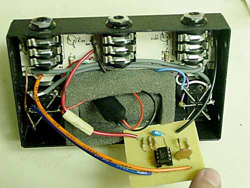
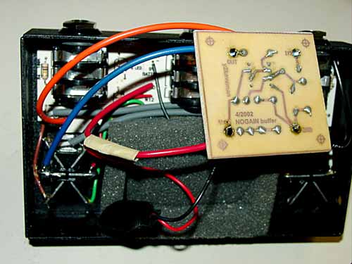
16. Here is a photo of the complete hook up of the buffer inside the pedal. Here's another with the back side of the PC board. Here's the color coding of the wires I ran to and from the buffer:
17. After soldering the wiring, I was ready to test. Hooked it up, and with the help of a friend, did a quick A/B between running the switch and bypassing it completely. There was a noticeable difference in sound, not mind-blowing, but definitely noticeable. The guitar's high-end could be heard much more clearly, and the guitar sounded more "hi-fi" somehow, that is, there was a noticeable increase in clearness and "headroom". Also, there was very little to no bleed between channels.
18. After some more testing and A/B'ing, we noticed that there was some serious pops and clicks upon activating either footswitch. I did notice the circuit already included a 100K tie-down resistor to ground to eliminate popping, which works fine on the unbuffered version (my friend has one I haven't modded yet to compare the two). I then realized my circuit didn't have an output capacitor that many designs have, which is used to block DC at the output. The combination of the capacitor and the 100K resistor form an R-C filter circuit which reduces the popping sound. So I used my Dremel drill press to do some work. First, I severed the trace on the Morley board which connects to the jack output. Next, I drilled an additional hole for the 100K tiedown resistor. Then I wired a 10uf electrolytic capacitor in series, with the positive side facing towards the buffer output, and the negative side connecting to the output jack. The final step was to resolder the 100K resistor from the negative side of the capacitor to ground. This is how it looked when I finished. (NOTE: as of 4/15/2002, this step will no longer be necessary, as I have re-designed my circuit to include the output coupling capacitor on the Buffer board itself.)
More steps would go here...but not likely soon added!
I also wanted to find out if I could incorporate a gain-control into the design, to offer greater than unity gain so that the "buffer" could be used as a volume boost. So I designed another version which I'll post soon.
Morley© is a registered trademake ok Sound Enhancements, Inc., 185 Detroit
Street Cary IL 60013.